
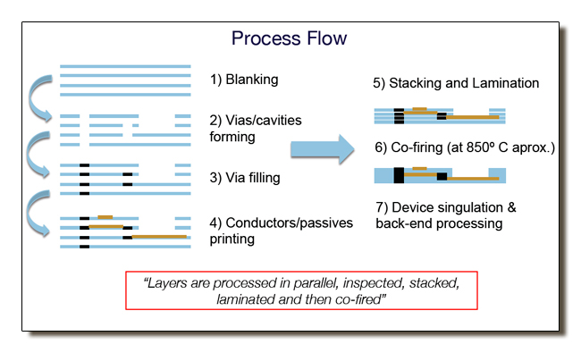
The fabrication of multi-layer circuits in LTCC technology consists on the following steps:
1. Blanking & Pre-conditioning: The LTCC tape is blanked at the process coupon size and pre-conditioned (if necessary) in a convection oven.
2. Via hole / Cavity forming: Registration and via holes are mechanically punched. Arbitrarily shaped cavities and windows can also be formed using a rectangular punching tool.
3. Via filling: Via holes are filled using a porous stainless-steel print nest by pulling via fill paste through the holes using a vacuum pump.
4. Conductor/passives printing: Conductors and passives are deposited using screen printing techniques. High resolution line width down to 80µm can be achieved using high-quality screens.
The former steps are carried out for every layer of the circuit. Sheets are inspected after each step using an automated optical metrology system. The following steps are carried out for each fabricated coupon:
5. Stacking: Layers are stacked and tacked using the registration holes created at the beginning of the process.
6. Lamination: The stack-up is laminated using an isostatic press in order to guarantee maximum process repetibility and avoid de-lamination.
7. Co-Firing: The laminated coupon is finally fired in a sintering oven. Excellent profile control and temperatura homogeneity inside the process chamber are essential in order to guarantee maximum shrinkage control and highest process yield.
8. Singulation: If multiple devices are fabricated on the same coupon, the components can be singulated using a dicing saw. Singulation can also be done after lamination (i.e. before sintering).
9. Post-processing: Die attach, wire bonding, SMD or flip-chip assembly are typical back-end processes that can be eventually carried out. Additional post-firing steps or fine-line photolithography can also be performed at this point.